
Ohio State opens $20M semiconductor cluster
The new Microelectronics Innovation and Technology Cluster aims to shorten the path from lab research to commercial manufacturing for defense and industry partners.
By Dylan Moore ·
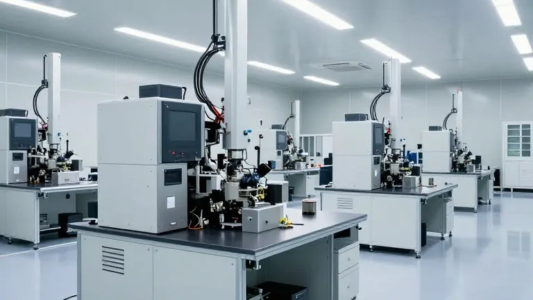
The Ohio State University opened a new semiconductor research facility on Oct. 20, adding capabilities designed to speed up the transition of technology from academic labs to manufacturing lines. The expansion allows researchers and industry partners to test devices at scales closer to commercial production, reducing the time required to move new materials to market.
The Microelectronics Innovation and Technology Cluster, known as MITEC, integrates existing resources across two campus locations. It connects the Nanotech West Lab with the Semiconductor Epitaxy and Analysis Laboratory. This setup creates a single environment for collaborative development and rapid prototyping.
The project required a total investment of more than $20 million. Approximately $16 million came from the Midwest Microelectronics Consortium, a regional innovation hub designated by the Department of War. The remaining $4.5 million came from a joint infrastructure investment by Ohio State and the Ohio Department of Higher Education. These funds paid for new equipment and facility upgrades.
MITEC is operated by the Institute for Materials and Manufacturing Research. Steven Ringel, a Distinguished University Professor and senior associate vice president for research, leads the cluster. He stated that the new capabilities aim to support device development for both defense and commercial applications. He described the partnership with the consortium as a key step for the Midwest's compound semiconductor sector.
John M. Horack, vice president for research, emphasized the university's role in applying knowledge beyond the classroom. He noted that a core part of the land-grant mission is sharing new discoveries with students. He added that the university is committed to translating research into solutions that drive economic growth. He summarized the goal by saying, “It’s one thing to demonstrate something in a lab. It’s another thing to do it at scale.”
The facility supports work on wide bandgap semiconductors used in high-power and high-speed electronics. It also handles narrow bandgap semiconductors required for infrared sensing. These materials are critical for modern defense systems and commercial electronics. The integrated environment allows for flexible testing of these materials.
Workforce development programs are already active under the new structure. MMEC-sponsored fellowships provide undergraduate and graduate students with hands-on experience. Students work in the cleanroom at Nanotech West Lab. They receive training from experienced staff while helping to develop new technologies.
Matt Casto, CEO of the Midwest Microelectronics Consortium, described Ohio State as a strategic partner in strengthening the domestic supply chain. He said the cluster brings together expertise and advanced facilities to accelerate technology development. He noted that expanding access to these tools helps bridge the gap between research and real-world applications.
The cluster is designed to support both small and large industry partners. It focuses on national defense technology development as a primary use case. The infrastructure is built to handle wafer sizes and processes that are compatible with industrial manufacturing standards. This alignment with commercial production metrics is central to the project's design.
The ribbon-cutting ceremony marked the completion of the physical upgrades. The facility is now operational for collaborative projects. Students and researchers have begun using the new equipment. The cluster continues to serve as a central node for the regional microelectronics ecosystem.
Source: Ohio State News